SOUND ManualSCSP / DSP Assembler User's Manual
BackForward
SCSP / DSP Assembler User's Manual

6. dAsms programming guide


■ Programming overview

When coding the dAsms source code, you do not need to be aware of pipeline processing, and you can write all commands in a sequential processing manner. In particular,

  1. Preparation of data required for calculation ( LDI / LDY / LDA )
  2. Description of multiplication / addition formula ( @ ... )
  3. Specifying the store destination ( > )

Consider the procedure of 1 as one unit processing, extract an appropriate partial function from the signal flow diagram, apply it to this unit processing, and describe the partial source code. The source code is written by repeating this in the order of processing.

The following explains how to code a DSP program in dAsms with a relatively simple concrete example.

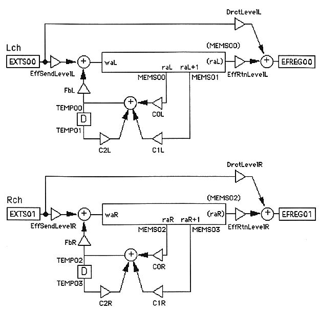
In the following program example, let's use the external extended inputs EXTS00 and EXTS01 that can input CD Audio etc. as Lch and Rch inputs, respectively, and output the results of delay (echo) processing independently for Lch and Rch to EFREG00 and EFREG01, respectively. It is to be.

■ Signal flow diagram

■ Coding procedure

1. Definition of coefficient symbol (#COEF)

1-1 Definition of coefficients related to level attenuation

As a coefficient related to level attenuation

Send level to delay : EffSendLevel L / R
Direct signal level : DrctLevel L / R
Return level from delay : EffRtnLevel L / R
Delay signal feedback level : FbL / R

Is defined. Level attenuation is defined in percentage notation, assuming that a level resolution of about 1% is sufficient. For the definition format, refer to " ■ Definition of coefficient / address symbol ". The definition description on the dAsms source code is as follows. The initial value is an example.

-------------------------------------------------- ---
     EffSendLevel L =% 100
     EffSendLevelR =% 100
     DrctLevelL =% 50
     DrctLevelR =% 50
     EffRtnLevelL =% 75
     EffRtnLevelR =% 75
     FbL =% 50
     FbR =% 50
-------------------------------------------------- ---

1-2 Definition of feedback filter-related coefficients

As the coefficient of the first-order IIR filter that serves as the feedback path for the delay signal, which can be seen in the signal flow diagram.

     C0L / R
     C1L / R
     C2L / R

Is defined. The filter coefficient is defined in decimal notation, assuming that it is given as a value normalized to 1. Considering an appropriate cutoff frequency, the definition description on the dAsms source code is as follows.

     C0L = 0.40893
     C0R = 0.40893
     C1L = 0.40893
     C1R = 0.40893
     C2L = 0.18164
     C2R = 0.18164

2. Definition of address constant symbol (#ADRS)

2-1 Definition of write and read addresses to the delay ring buffer
In the signal flow diagram, the rectangle in the center of each part of Lch / Rch represents the delay. The delay is created by the ring buffer, and the delay time is proportional to the difference between the write and read addresses. One address corresponds to one sample of delay. As an address constant

     waL / R
     raL / R

Is defined. For these address constant symbols, it is possible to give the address on the ring buffer as an initial value in hexadecimal or decimal integer, but in dAsms, the notation that the address is converted to time (millisecond) can be used. Considering an appropriate delay time, the definition description on the dAsms source code is as follows.

-------------------------------------------------- --------------
     waL = ms0.0
     raL = ms149.9
     waR = ms150.0
     raR = ms249.9
-------------------------------------------------- --------------

3. Description of program part (#PROG)

3-1 Preparation of data on the Lch side
Looking at the signal flow diagram, we can see that memory access (reading from the ring buffer) is required to obtain the data required for the operation. The address on the ring buffer to be read is

     raL
     raL + 1

is. However, since these addresses are only relative positions on the ring buffer, the address description element "DEC" is added to the "..." part of the external memory read parameter "MR [...]". "DEC" represents a counter that is decremented by 1 for each sample, and the ring buffer operation is realized only by adding this to the address description element. Data read from the positions of raL and raL + 1 on the ring buffer, respectively.

     MEMS00
     MEMS01

Assuming that it is loaded into, the above can be expressed in the dAsms source code as follows.

     LDI MEMS00, MR [raL + DEC]
     LDI MEMS01, MR [raL + DEC + 1]

For reference, the addresses on the ring buffer accessed by the above two "MR [...]" are one address for each sample by the action of "DEC" while keeping the distance of one address from each other. It shifts in the lower direction.

3-2 Calculation of filter part for Lch side feedback
Once the required data is ready, the next step is to write a description for performing operations using those data. The procedure for calculating the first-order IIR filter, which is the feedback path for the delay signal, is as follows.

  1. Multiply the value loaded on MEMS00 by the coefficient C0L.

  2. Multiply the value loaded in MEMS01 by the coefficient C1L and add it to the result of (1).

  3. Multiply the value of TEMP01 by the coefficient C2L and add it to the result of (2).

  4. Store the result of (3) in TEMP00.

The important thing here is that TEMP is a ring buffer. In TEMPxx, its subscript xx represents a relative address as a ring buffer, and the data stored in TEMP00 will appear in TEMP01 in the next sample. In (3) and (4) above, this is used to realize a delay for one sample.

In dAsms, the description method of the calculation formula is a little special due to the characteristics of the SCSP / DSP hardware that it targets. The contents of (1) to (4) above can be expressed in the dAsms source code as follows.

-------------------------------------------------- ------------------------
     @ TEMP01 * C2L + (MEMS01 * C1L + (MEMS00 * C0L +))> TEMP00
-------------------------------------------------- ------------------------

Thus, note that in order to describe continuous multiplication and addition as in (1)-(3) above, the actual order of each multiplication and the descriptive order must be reversed.

3-3 Writing to the Lch side ring buffer
From the signal flow diagram,

  1. The value of the input EXTS00 multiplied by the coefficient EffSendLevelL

  2. The value stored in TEMP00 in 3-2 (4) multiplied by the coefficient FbL

You can see that you should write the sum of the two to the ring buffer. The write address on the ring buffer is waL and uses the address description element "DEC" as in MR [...] in 3-1. The above contents can be expressed on the dAsms source code as follows.

-------------------------------------------------- ------------------------
     @ TEMP00 * FbL + (EXTS00 * EffSendLevelL +)> MW [waL + DEC]
-------------------------------------------------- ------------------------

3-4 Lch output data generation and writing to EFREG
From the signal flow diagram,

  1. Data read from the address raL on the ring buffer multiplied by the coefficient EffRtnLevelL

  2. The value of the input EXTS00 multiplied by the coefficient DrctLevelL

You can see that the sum of the two should be stored in EFREG00. Here, the data required for multiplication in (a) (read from the ring buffer) is loaded in MEMS00 in 3-1 and is used. The above contents can be expressed on the dAsms source code as follows.

-------------------------------------------------- ------------------------
     @ EXTS00 * DrctLevelL + (MEMS00 * EffRtnLevelL +)> EFREG00
-------------------------------------------------- ------------------------

This completes the description of the source code on the Lch side.

3-5 Rch side source code description
The function of this program example is stereo (L / R independent) delay, but as you can see from the signal flow diagram, the processing content on the Rch side is the same as that on the Lch side. However, the coefficient / address constant symbol name, register name, etc. used are different. Therefore, if you copy and paste the Lch side source code described up to the previous section and rewrite only the changed part, it will be the Rch side source code.

3-6 Finished coding
This completes the description of the source code of this program example. The overall picture of the source code according to " 3. Source code configuration" is as follows.

-------------------------------------------------- ------------------------
     'dAsms sample program.
     'Function: L / R independent delay
     'CD Lch Direct + Delayed-> EFREG00
     'CD Rch Direct + Delayed-> EFREG01
     #COEF

     'Levels
     EffSendLevel L =% 100
     EffSendLevelR =% 100
     DrctLevelL =% 50
     DrctLevelR =% 50
     EffRtnLevelL =% 75
     EffRtnLevelR =% 75
     FbL =% 50
     FbR =% 50

     'FilterCoefs
     C0L = 0.40893
     C0R = 0.40893
     C1L = 0.40893
     C1R = 0.40893
     C2L = 0.18164
     C2R = 0.18164

     #ADRS
     waL = ms0.0
     raL = ms149.9
     waR = ms150.0
     raR = ms249.9

     #PROG

     'Lch
     LDI MEMS00, MR [raL + DEC]
     LDI MEMS01, MR [raL + DEC + 1]
     @ TEMP01 * C2L + (MEMS01 * C1L + (MEMS00 * C0L +))> TEMP00
     @ TEMP00 * FbL + (EXTS00 * EffSendLevelL +)> MW [waL + DEC]
     @ EXTS00 * DrctLevelL + (MEMS00 * EffRtnLevelL +)> EFREG00

'Rch LDI MEMS02, MR [raR + DEC] LDI MEMS03, MR [raR + DEC + 1] @ TEMP03 * C2R + (MEMS03 * C1R + (MEMS02 * C0R +))> TEMP02 @ TEMP02 * FbR + (EXTS01 * EffSendLevelR +)> MW [waR + DEC] @ EXTS01 * DrctLevelR + (MEMS02 * EffRtnLevelR +)> EFREG01 #END -------------------------------------------------- ------------------------


BackForward
SOUND ManualSCSP / DSP Assembler User's Manual
Copyright SEGA ENTERPRISES, LTD., 1997