HARDWARE ManualSCSP User's Manual
BackForward
SCSP User's Manual / 4.3 Sound Source Register

Until now, "MDXSL" and "MDYSL" have been calculated by calculation, but from the slot numbers of the side to be modulated (modulator) and the side to be modulated (carrier), "MDXSL" is used using the parameter correspondence table in Table 4.16. You can derive the values for "and" MDYSL ".
Using the parameter table below, find "MDXSL" and "MDYSL" in Figure 4.33.

(1) Parameters to be set in slot 0
Slot 0 has a self-feedback configuration, so the carrier slot number and modulator slot number are "00". At this time, "MDXSL" and "MDYSL" are from the parameter table.

Latest sample. .. .. .. .. 20H
Past sample. .. .. .. 00H

It will be. As mentioned earlier, in the case of self-feedback, if the same generation is used for input, it may oscillate, so avoid this usage.

(2) Parameters to be set in slot 2
Slot 2 has a multi-input configuration.
First, when slot 1 is input, the carrier slot number is "02" and the modulator slot number is "01". At this time, "MDXSL" and "MDYSL" are from the parameter table.

Latest sample. .. .. .. .. 1FH
Past sample. .. .. .. 3FH

It will be.

Next, when slot 0 is input, the carrier slot number will be "02" and the modulator slot number will be "00". At this time, "MDXSL" and "MDYSL" are from the parameter table.

Latest sample. .. .. .. .. 1EH
Past sample. .. .. .. 3EH

It will be.

(3) Parameters to be set in slot 3
Slot 3 takes the output of slot 2 as input. Therefore, the carrier slot number is "03" and the modulator slot number is "02". At this time, "MDXSL" and "MDYSL" are from the parameter table.

Latest sample. .. .. .. .. 1FH
Past sample. .. .. .. 3FH

It will be.

Table 4.16 Relationship between MDXSL / MDYSL and slots

MDXSL / MDYSL carrier slot number Parameter value 00 01 02 03 04 05 06 07 08 09 10 11 12 13 14 15 (SAMPLE) Latest Past Modulation Slot Number SLOT 00-31 20H 00H 00 01 02 03 04 05 06 07 08 09 10 11 12 13 14 15 21H 01H 01 02 03 04 05 06 07 08 09 10 11 12 13 14 15 16 22H 02H 02 03 04 05 06 07 08 09 10 11 12 13 14 15 16 17 23H 03H 03 04 05 06 07 08 09 10 11 12 13 14 15 16 17 18 24H 04H 04 05 06 07 08 09 10 11 12 13 14 15 16 17 18 19 25H 05H 05 06 07 08 09 10 11 12 13 14 15 16 17 18 19 20 26H 06H 06 07 08 09 10 11 12 13 14 15 16 17 18 19 20 21 27H 07H 07 08 09 10 11 12 13 14 15 16 17 18 19 20 21 22 28H 08H 08 09 10 11 12 13 14 15 16 17 18 19 20 21 22 23 29H 09H 09 10 11 12 13 14 15 16 17 18 19 20 21 22 23 24 2AH 0AH 10 11 12 13 14 15 16 17 18 19 20 21 22 23 24 25 2BH 0BH 11 12 13 14 15 16 17 18 19 20 21 22 23 24 25 26 2CH 0CH 12 13 14 15 16 17 18 19 20 21 22 23 24 25 26 27 2CH 0DH 13 14 15 16 17 18 19 20 21 22 23 24 25 26 27 28 2EH 0EH 14 15 16 17 18 19 20 21 22 23 24 25 26 27 28 29 2FH 0FH 15 16 17 18 19 20 21 22 23 24 25 26 27 28 29 30 30H 10H 16 17 18 19 20 21 22 23 24 25 26 27 28 29 30 31 31H 11H 17 18 19 20 21 22 23 24 25 26 27 28 29 30 31 00 32H 12H 18 19 20 21 22 23 24 25 26 27 28 29 30 31 00 01 33H 13H 19 20 21 22 23 24 25 26 27 28 29 30 31 00 01 02 34H 14H 20 21 22 23 24 25 26 27 28 29 30 31 00 01 02 03 35H 15H 21 22 23 24 25 26 27 28 29 30 31 00 01 02 03 04 36H 16H 22 23 24 25 26 27 28 29 30 31 00 01 02 03 04 05 37H 17H 23 24 25 26 27 28 29 30 31 00 01 02 03 04 05 06 38H 18H 24 25 26 27 28 29 30 31 00 01 02 03 04 05 06 07 39H 19H 25 26 27 28 29 30 31 00 01 02 03 04 05 06 07 08 3AH 1AH 26 27 28 29 30 31 00 01 02 03 04 05 06 07 08 09 3BH 1BH 27 28 29 30 31 00 01 02 03 04 05 06 07 08 09 10 1CH 3CH 28 29 30 31 00 01 02 03 04 05 06 07 08 09 10 11 1DH 3DH 29 30 31 00 01 02 03 04 05 06 07 08 09 10 11 12 1EH 3EH 30 31 00 01 02 03 04 05 06 07 08 09 10 11 12 13 1FH 3FH 31 00 01 02 03 04 05 06 07 08 09 10 11 12 13 14
MDXSL / MDYSL carrier slot number Parameter value 16 17 18 19 20 21 22 23 24 25 26 27 28 29 30 31 (SAMPLE) Latest Past Modulation Slot Number SLOT 00-31 20H 00H 16 17 18 19 20 21 22 23 24 25 26 27 28 29 30 31 21H 01H 17 18 19 20 21 22 23 24 25 26 27 28 29 30 31 00 22H 02H 18 19 20 21 22 23 24 25 26 27 28 29 30 31 00 01 23H 03H 19 20 21 22 23 24 25 26 27 28 29 30 31 00 01 02 24H 04H 20 21 22 23 24 25 26 27 28 29 30 31 00 01 02 03 25H 05H 21 22 23 24 25 26 27 28 29 30 31 00 01 02 03 04 26H 06H 22 23 24 25 26 27 28 29 30 31 00 01 02 03 04 05 27H 07H 23 24 25 26 27 28 29 30 31 00 01 02 03 04 05 06 28H 08H 24 25 26 27 28 29 30 31 00 01 02 03 04 05 06 07 29H 09H 25 26 27 28 29 30 31 00 01 02 03 04 05 06 07 08 2AH 0AH 26 27 28 29 30 31 00 01 02 03 04 05 06 07 08 09 2BH 0BH 27 28 29 30 31 00 01 02 03 04 05 06 07 08 09 10 2CH 0CH 28 29 30 31 00 01 02 03 04 05 06 07 08 09 10 11 2DH 0DH 29 30 31 00 01 02 03 04 05 06 07 08 09 10 11 12 2EH 0EH 30 31 00 01 02 03 04 05 06 07 08 09 10 11 12 13 2FH 0FH 31 00 01 02 03 04 05 06 07 08 09 10 11 12 13 14 30H 10H 00 01 02 03 04 05 06 07 08 09 10 11 12 13 14 15 31H 11H 01 02 03 04 05 06 07 08 09 10 11 12 13 14 15 16 32H 12H 02 03 04 05 06 07 08 09 10 11 12 13 14 15 16 17 33H 13H 03 04 05 06 07 08 09 10 11 12 13 14 15 16 17 18 34H 14H 04 05 06 07 08 09 10 11 12 13 14 15 16 17 18 19 35H 15H 05 06 07 08 09 10 11 12 13 14 15 16 17 18 19 20 36H 16H 06 07 08 09 10 11 12 13 14 15 16 17 18 19 20 21 37H 17H 07 08 09 10 11 12 13 14 15 16 17 18 19 20 21 22 38H 18H 08 09 10 11 12 13 14 15 16 17 18 19 20 21 22 23 39H 19H 09 10 11 12 13 14 15 16 17 18 19 20 21 22 23 24 3AH 1AH 10 11 12 13 14 15 16 17 18 19 20 21 22 23 24 25 3BH 1BH 11 12 13 14 15 16 17 18 19 20 21 22 23 24 25 26 1CH 3CH 12 13 14 15 16 17 18 19 20 21 22 23 24 25 26 27 1DH 3DH 13 14 15 16 17 18 19 20 21 22 23 24 25 26 27 28 1EH 3EH 14 15 16 17 18 19 20 21 22 23 24 25 26 27 28 29 1FH 3FH 15 16 17 18 19 20 21 22 23 24 25 26 27 28 29 30

* How to read the table
First, find the slot number on the carrier side, and then find the slot number of the modulator that is input to it. Find the corresponding number of samples in the side column.

Next, I will explain about "MDL" (Modulation Level).
"MDL" is a parameter that sets the degree of modulation (the degree of modulation) by the modulation signal applied to the modulation inputs X and Y. Increasing this value will increase the degree of frequency modulation, and decreasing it will decrease the degree of frequency modulation (Fig. 4.32).

Figure 4.32 MDL modulation
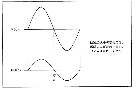
This section describes the degree of modulation by the "MDL" setting value. Table 4.15 shows that the modulation factor becomes ± nπ depending on the setting value of "MDL".
The averaging unit averages each data in the sound slots input to the modulation inputs X and Y. Assuming that the data input to X is XD, the data input to Y is YD, and the output of the averaging calculation unit is ZD, it can be expressed as the following formula.


ZD = (XD + YD) ÷ 2

This ZD is level adjusted by "MDL" and sent to the slot's address pointer (phase adder).

Figure 4.33 Maximum displacement due to waveform read address
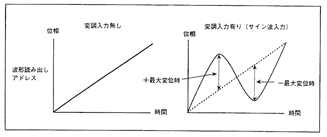
In FM speech synthesis, the time-phase function is linear when no modulation waveform is added. However, when a modulated waveform is added, the displacement of the modulated waveform is added, so the time-phase waveform that was linear becomes non-linear (non-linear). This displacement is maximized when ZD has a maximum value of ±. The degree of modulation of MDL represents the displacement (maximum displacement) of the waveform address when ZD takes ± maximum value with the waveform data (sine wave) set to 1 cycle = 1K word.

Table 4.10 Maximum address displacement due to register settings
MDL [3: 0]
 0-4
 Five
 6
 7
 8
 9
 A
 B
 C
 D
 E
 F
 Address maximum displacement ±
0 32 64 128 256 512 1024 2048 4096 8192 16384 32768

Comparing Table 4.16 and Table 4.10, we get the relationship π = 512 (when MDL = AH). In Table 4.16, the waveform data (sine wave) is considered to be 1 cycle = 1K word (1024 words), but the mathematical expression method defines the length of one waveform cycle as 2π. Therefore, in this FM speech synthesis, since the sine wave of 1 cycle = 1K word is used, 512 of the maximum address displacement can be expressed by π. The expression method using π is valid only when one cycle of the waveform data is 1K word. In other cases, use the expression method by address displacement in Table 4.10.

When performing FM speech synthesis, make sure to have waveform data for 3 cycles. The reason is that address displacement occurs. In SCSP hardware, it is necessary to store the waveform data in the memory up to the 1K word address displacement (MDL = "AH"), but for those exceeding 1K word, the hardware automatically clips the data. Therefore, it is not necessary to store more waveform data than 1K word.

Figure 4.34 Address displacement during FM synthesis

When performing FM speech synthesis, put extra data for the address displacement. Basically, if it is ± π, there is no problem in operation by setting the waveform data for π before "SA" and after "LEA" (when PLFO is not used). However, it is preferable to put the data for 3 cycles as shown in Fig. 4.34.

* About clipping process
This is related to the address displacement described earlier. Since the range of address displacement changes by a maximum of ± 32768 addresses depending on "MDL", waveform data for 32 cycles (32K words) is required before and after one basic waveform cycle (1K words), for a total of 65K words. It requires a lot of memory.
Therefore, in SCSP, when the displacement exceeds 1K word, clipping (processing to prevent it from exceeding) is performed and the displacement is returned to 0. As a result, no matter how much the displacement is, if there is waveform data of 3K words in total, it can be sufficiently handled.
Also, since the effective address bit prepared for displacement is 10 bits, clipping processing will be performed.

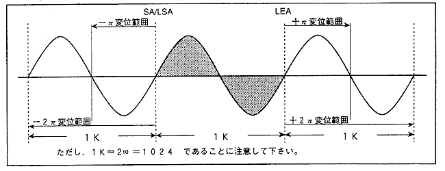
Figure 4.35 Wave data during clipping processing

As shown in Fig. 4.35, even if the preliminary waveform is exceeded after displacement, it is returned to 0 when the phase exceeds 2π.

Next, I will explain how to set up the FM configuration (algorithm) in SCSP. Since SCSP slots basically have a 2-input, 1-output structure, the maximum number of slots that can be connected (modulated) to one slot is two. ..

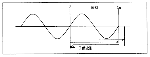
Figure 4.36 Number of slot connections

Modulation is possible up to two, as shown in Figure 4.36. Also, considering that the modulation data (source) is brought from the sound stack, SCSP can create FM configurations as shown in Fig. 4.37, Fig. 4.38, Fig. 4.39, and Fig. 4.40.
(Fig. 4.37 shows a configuration in which a slot with self-feedback is modulated by another slot, Fig. 4.38 shows multi-stage feedback including multiple slots, Fig. 4.39 shows combined feedback that combines multi-stage feedback and self-feedback, and Fig. 4.40. Represents a composite modulation type that modulates each slot with multi-stage feedback in a separate slot.)

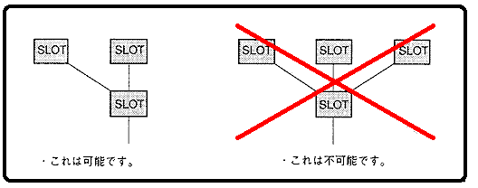
Figure 4.37 Self-feedback modulation

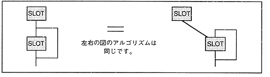
Figure 4.38 Multi-stage feedback
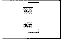
Figure 4.39 Combined feedback

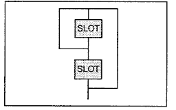
Figure 4.40 Composite modulation

Figure 4.41 and Figure 4.42 show specific examples of the basic FM configuration. Please use it as a reference when performing FM speech synthesis. The upper two lines of each slot represent the modulation input, and the lower line represents the slot output.
Also, in Fig. 4.41 and Fig. 4.42, it seems that only one slot is connected to each other, so actually connect the broken line part as well.

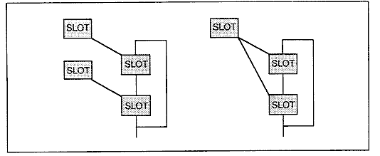
Figure 4.41 FM configuration algorithm pattern 1

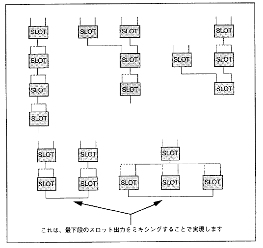
Figure 4.42 FM configuration algorithm pattern 2

In FM speech synthesis, the top slot has nothing to connect to without self-feedback. In such a case, set the value of "MDL" from 0B "to" 4B "and set the modulation degree to" 0 ". This allows the modulation input to be set to" 0 ". ..

* Definition of top slot
The top slot is the top slot of each tower in the algorithm. In Figure 4.43, there are three towers: S0 tower, S1, S2 tower, and S3, S4, S5, S6 tower. These top slots are S0, S1, S6.

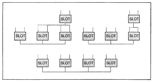
Figure 4.43 7-slot FM configuration
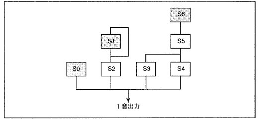

BackForward
HARDWARE ManualSCSP User's Manual
Copyright SEGA ENTERPRISES, LTD., 1997