 ★ HARDWARE Manual ★ SCU User's Manual
▲ Back | Forward ▼
SCU User's Manual Chapter 4 DSP Control
■ 4.1 DSP internal block diagram
- Figure 4.1 shows the internal block diagram of the DSP.
- Figure 4.1 DSP internal block diagram
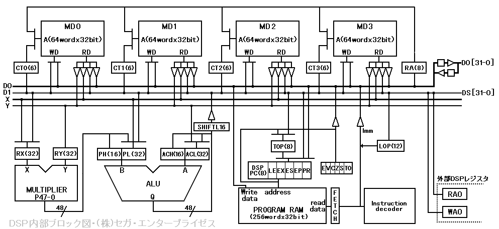
- ● ALU
- An arithmetic unit that can output up to 48 bits. Normal calculation is executed in 32bit. Only the product-sum operation is a 48-bit operation.
- ● MULTI PLIER
- It is a multiplier that obtains 64bit results with 32bit x 32bit and outputs the lower 48bits. Of the 48-bit data, the upper 16 bits are stored in PH (see below) and the lower 32 bits are stored in PL (see below).
- ● TOP (W)
- An 8-bit register that stores the start address. In JUMP instruction, subroutine execution processing, etc., the start address is stored in this register and the processing is executed.
- ● LOP (W)
- A 12-bit register that stores a loop counter. Set the number of loops in the iterative execution process of one instruction.
- ● CT0-3 (W)
- This is a 6-bit register that stores the access address of data RAM0-3.
- ● MD0-3 (R / W)
- Data RAM A 32-bit data port that stores 0-3 data. It has 64 data ports for each data RAM.
- ● RA (W)
- Address storage register for accessing data RAM. This register is 8 bits. The upper 2 bits store the RAM specification number (0-3), and the lower 6 bits store the RAM access address.
- ● RX (W)
- A 32-bit X-bus connection register that stores multiplier input data.
- ● RY (W)
- A 32-bit Y-bus connection register that stores multiplier input data.
- ● PH (W)
- This register stores the upper 16 bits of the 48-bit multiplier output data. It is also an input data storage register that stores the upper 16 bits of the input data B (48 bits) of the ALU arithmetic unit.
- ● PL (W)
- A register that stores the lower 32 bits of the 48-bit multiplier output data. It is also an input data storage register that stores the lower 32 bits of the input data B (48 bits) of the ALU arithmetic unit.
- ● ACH (W)
- This register stores the upper 16 bits of the 48 bit data that represents the ALU calculation result. It is also an input data storage register that stores the upper 16 bits of the input data A (48 bits) of the ALU arithmetic unit.
- ● ACL (W)
- This register stores the lower 32 bits of the 48 bit data that represents the ALU calculation result. It is also an input data storage register that stores the lower 32 bits of the input data A (48 bits) of the ALU arithmetic unit.
- ● D0 bus
- It is a 32-bit data bus for accessing the outside. It operates at 28MHz. Used to access the main CPU.
- ● X bus, Y bus
- It is a 32-bit data bus for obtaining arithmetic input data. It operates at 14MHz.
- ● RA0 (W)
- External → 32-bit external address register used for DSP DMA transfer. Since the value is taken in units of 4 bytes, shift the external address to the right by 2 bits and set it.
- ● WA0 (W)
- This is a 32-bit external address register used for DSP → external DMA transfer. Since the value is taken in units of 4 bytes, shift the external address to the right by 2 bits and set it.
▲ Back | Forward ▼
★ HARDWARE Manual ★ SCU User's Manual
Copyright SEGA ENTERPRISES, LTD., 1997