VDP2 displays the scroll screen data while reading it from VRAM in synchronization with the TV scan. VRAM access during the display period repeats the cycle with 4 or 8 accesses as the operation unit (1 cycle). When the TV screen mode is normal mode, 8 accesses are in one cycle. Also, in high resolution mode or dedicated monitor mode, four accesses are one cycle. There are 10 types of VRAM access performed during one cycle.
- Normal scroll screen pattern name data read access
- Character pattern data read access or bitmap pattern data read access on the normal scroll screen
- Vertical cell scroll table data read access for NBG0 and NBG1
- Read / write access by CPU
- Do not access
- RBG0 pattern name data read access
- RBG0 character pattern data read access or bitmap pattern data read access
- RBG0 coefficient table data read access
- RBG1 pattern name data read access
- RBG1 character pattern data read access
It is necessary to specify the timing of VRAM access in 1 to 5 above for each bank of VRAM-A0, VRAM-A1, VRAM-B0, and VRAM-B1 in one cycle. The specification is made by writing a 4-bit value called an access command corresponding to each VRAM access type to the VRAM cycle pattern register. Since each of the VRAM accesses from 6 to 8 occupies the timing of the entire cycle, only one type can be specified for one bank. The specification is made by writing the value corresponding to each VRAM access type to the rotation databank specification bit of the RAM control register. The setting of the VRAM cycle pattern register of the bank for which VRAM access in 6 to 8 is specified is invalid. VRAM access in 9. and 10. occupy the timing of the entire cycle, respectively, 9 is fixed to VRAM-B1 and 10. is fixed to VRAM-B0. The specifications of 9. and 10. are automatically made when RBG1 is displayed, and at that time, the setting of the VRAM cycle pattern register of VRAM-B0 and VRAM-B1 becomes invalid.
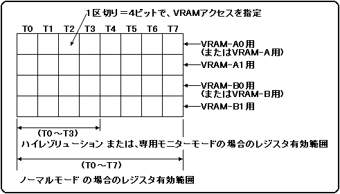
The VRAM cycle pattern register has registers corresponding to each bank of VRAM-A0, VRAM-A1, VRAM-B0, and VRAM-B1. If VRAM is not split in two, the register for VRAM-A0 will be used for VRAM-A, the register for VRAM-B0 will be used for VRAM-B, and the register for VRAM-A1 and VRAM-B1 will not be used. Hmm. The registers corresponding to each bank are divided into eight access timings from T0 to T7, and access is performed in order from the VRAM access indicated by the access command specified in the T0 bit. When the TV screen is in normal mode, all of T0 to T7 are enabled. In high resolution mode or dedicated monitor mode, only T0 to T3 are valid, and T4 to T7 are ignored. Figure 3.2 shows the VRAM cycle pattern registers used during one cycle. Figure 3.2 VRAM cycle pattern register
Be sure to set "Do not access" for the access timing left over after specifying the VRAM access required for display. Also, if the VRAM access address specified in the VRAM cycle pattern register is not an address in the specified bank, access will not be performed and correct screen display will not be possible.