Wait cycles are inserted into the CPU until, but in the case of write access, wait cycles are not inserted up to 2 word write accesses.
VRAM access by the CPU can only be specified in units of access to VRAM-A or access to VRAM-B, not in units of banks.
To specify VRAM access by the CPU for VRAM that is not divided into two, specify the CPU read / write access command in the VRAM cycle pattern register at the timing of access. At this time, it is the same even if you specify an access command that does not access instead of the CPU read / write access command. Also, when the access command for the screen (pattern name data read, character pattern data read, or bitmap pattern data read) that is set not to be displayed is set in the screen display enable register, CPU read / write access is set. Become. For details on the screen display enable register, see " 4.1 Screen Display Control."
If you specify a CPU read / write or no access command for all access timings of VRAM that is not divided into two, CPU access is possible at any time during the screen display period. You can use this to use one of the VRAMs as auxiliary work RAM. Also, by switching the VRAM used to display the picture like a frame buffer, you can display the picture while rewriting it at high speed.
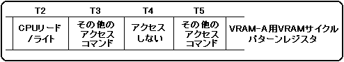
For example, if VRAM-A is not divided into two banks, the VRAM cycle pattern register specification for CPU read / write access to T2 and T4 is shown in Figure 3.6. Figure 3.6 Example of CPU read / write access specification when VRAM is not divided into 2 banks
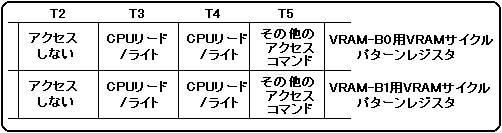
When setting CPU read / write access for VRAM divided into two, set the CPU read / write access command in both the VRAM cycle pattern registers for bank 0 and bank 1 at the timing of access. Must be. In addition, you must specify the access command not to access both the bank 0 and bank 1 registers at the timing immediately before the CPU read / write access command is set. However, if you want to specify CPU read / write access at consecutive timings, you only need to specify it at the timing immediately before the timing at the beginning of the continuous access. For example, when dividing VRAM-B into two, the specification of the VRAM cycle pattern register when performing continuous CPU read / write access to T4 and T5 is as shown in Fig. 3.7. Figure 3.7 Example of CPU read / write access specification when dividing VRAM into 2 banks