HARDWARE ManualSCU User's Manual
BackForward
SCU User's Manual / Chapter 2 Operation Description

◆ Specific usage example

● Direct mode
Consider the case of transferring 1KByte from address 2000000H (A-Bus area) to address 6000000H (work RAM) with level 0 DMA. You can execute DMA (Direct Mode) by following the steps below.

  1. Writes the read address (2000000H) to the read address register D0R.
    (The read address is loaded from the CPU to address 25FE0000H.)

  2. Writes the write address (6000000H) to the write address register D0W.
    (Loads the write address from the CPU to address 25FE0004H.)

  3. Writes the number of transferred bytes (400H) to the number of transferred bytes register D0C.
    (Loads the number of bytes transferred from the CPU to address 25FE0008H.)

  4. Writes the address addition value (101H) to the address addition value register D0AD.
    (The address addition value is loaded from the CPU to the address 25FE000CH. The details of the address addition value are described in the address addition value in this section. In normal DMA, specify 101H as the address addition value.)

  5. Set the DMA mode to 0, set the address update bit and the DMA activation factor as necessary, and write to the mode / address update / DMA activation factor register D0MD. For example, if the address update is set to the retention mode and V-blank-IN is the activation factor, 0 is written to D0MD.
    (Loads 0 from the CPU to address 25FE0014H.)

  6. When the DMA enable bit is set to 1 and the activation factor set in (5) occurs, DMA is activated and data of 1KByte at level 0 from the address 2000000H (A-Bus area) to the address 6000000H (work RAM). To transfer.

  7. After the DMA is completed, the DMA is activated every time the activation factor set in (5) occurs. At that time, the operation depends on the values of the read address update bit (D0RUP) and the write address update bit (D0WUP). Figure 2.7 shows the difference in DMA operation depending on the address update bit.

However, (1) to (5) can be in any order. (When the startup factor is set to the DMA startup bit, DMA is started every time the DMA operation bit is set to 1 on the CPU.)

Figure 2.7 Differences in DMA operation depending on the address update bit

D0RUP = 0
When D0WUP = 0

D0RUP = 0
When D0WUP = 1

D0RUP = 1
When D0WUP = 0

D0RUP = 1
When D0WUP = 1

When the read address update bit is 0, the same address is referenced (read) both the first time and the second time. When the read address update bit is 1, the address referred to the second time will refer to the address next to the first time.
When the write address update bit is 0, writing is performed to the same address both the first time and the second time. When the write address update bit is 1, the second write is performed from the next address written the first time.

● Indirect mode
Indirect mode is used when you want to perform multiple DMA transfers with a single boot. In the indirect mode, instead of setting the register in the register as in the direct mode, the method is to access the register via RAM and execute DMA. As an example, consider the case where you want to perform the following three DMA transfers continuously at level 0 over the work RAM area (6000000H).

You can execute DMA (indirect mode) by following the steps below.

  1. As shown in Figure 2.8, data is written in longword units from the work RAM area (6000000H).

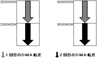
    Figure 2.8 Example of writing data

    6000000H ┏━━━━━━━━━━┓ ┐
    ┃ 20H ┃ │ ← (number of bytes transferred)
    ┠──────────┨ │
    ┃ 5C00000H ┃ │ (a) ← (transfer source address)
    ┠──────────┨ │
    ┃ 4000000H ┃ │ ← (forwarding address)
    600,000 CH ┣━━━━━━━━━━┫ ┘
    ┃ 10H ┃ │
    ┠──────────┨ │
    ┃ 6080000H ┃ │ (b)
    ┠──────────┨ │
    ┃ 5E00000H ┃ │
    6000018H ┣━━━━━━━━━━┫ ┘
    ┃ 15H ┃ │
    ┠──────────┨ │
    ┃ 6081000H ┃ │ (c)
    ┠──────────┨ │
    ┃ DA00000H ┃ │ ← 8000000H + 5A00000H
    6000024H ┣━━━━━━━━━━┫ ┘ (Exit code) (Forwarding address)
    ┃ ┃ 


  2. Writes the DMA parameter source address (6000000H) to the write address register (D0W).

  3. Writes the address addition value (101H) to the address addition value register D0AD.
    (The address addition value is loaded from the CPU to the address 25FE000CH. The details of the address addition value are described in the address addition value in this section. In normal DMA, specify 101H as the address addition value.)

  4. Set the DMA mode to 1, set the address update bit and DMA activation factor as necessary, and write to the mode / address update / DMA activation factor register D0MD. For example, if the address update is set to the retention mode and V-blank-IN is the starting factor, 1000000H is written to D0MD.
    (Loads 1000000H from the CPU to address 25FE0014H.)

  5. When the DMA enable bit is set to 1 and the activation factor set in (4) occurs, DMA is activated and the DMA transfers in (a) to (c) are executed in order until the DMA end code is detected. The DMA end code is a DMA indirect mode end notification code that exists only in the work RAM area, and DMA transfer continues unless this bit "1" is detected.

However, (1) to (4) can be in any order. The "read address register (D0R)" and "transfer byte register (D0C)" that had to be set in direct mode do not need to be set in indirect mode.
Furthermore, it is assumed that the following DMA transfer has been registered in the memory.

The contents from the work RAM area 6000000H at this time are as shown in Fig. 2.9.
The DMA is restarted every time the startup factor set in (5) occurs.

Figure 2.9 Contents of work RAM area
6000000H ┏━━━━━━━━━━┓
┃ 20H ┃
┠──────────┨
┃ 5C00000H ┃
┠──────────┨
┃ 4000000H ┃
600,000 CH ┣━━━━━━━━━━┫
┃ 10H ┃
┠──────────┨
┃ 6080000H ┃
┠──────────┨
┃ 5E00000H ┃
6000018H ┣━━━━━━━━━━┫
┃ 15H ┃
┠──────────┨
┃ 6081000H ┃
┠──────────┨
┃ DA00000H ┃
6000024H ┣━━━━━━━━━━┫ ┐
┃ 30H ┃ │
┠──────────┨ │
┃ 6090000H ┃ │ (d)
┠──────────┨ │
┃ 5000000H ┃ │
6000030H ┣━━━━━━━━━━┫ ┘
┃ 25H ┃ │
┠──────────┨ │
┃ 60A0000H ┃ │ (e)
┠──────────┨ │
┃ D1000000H ┃ │ ← 8000000H + 510000H
6000003CH ┣━━━━━━━━━━┫ ┘ (Exit code) (Forwarding address)
┃ ┃

When restarting, the operation differs depending on whether the DMA mode is retention mode or update mode. The indirect mode retention / update mode is recognized by the write address update bit.

<In retention mode (write address update bit = 0)>
After the first DMA transfer is completed, the address to access the parameter is held at 6000000H, so the DMA transfer of (A) to (C) is executed again.

<In update mode (write address update bit = 1)>
After the first DMA transfer is completed, the address to access the parameter is updated to 6000024H, so the DMA transfer of (D) to (E) is executed.

● Address addition value
Normally, DMA accesses continuous areas, but it is possible to access addresses at regular intervals by setting an address addition value. This function is effective when you want to change some of the parameters that are arranged consecutively, such as the VDP1 command table. As an example, suppose there are 32 blocks with addresses 5C00000H to 20H bytes in one table. Consider rewriting the parameters of the 8th byte of each block at once. Assuming that the parameter for change has an address of 6000000H to 40H bytes, when transferring with level 0 DMA, set it according to the following procedure and execute the transfer process.

  1. Writes the read address 6000000H to the read address register D0R.

  2. Writes the write address 5C00008H to the write address register D0W.

  3. Writes the number of transfer bytes 40H to the number of transfer bytes register D0C.

  4. Writes the address addition value 105H to the address addition value register D0AD.
    In this, the lower 3 bits (5 = 101B) indicate that the address is updated by 20H.

  5. Set the DMA mode to 0, set the address update bit and the DMA activation factor as necessary, and write to the mode / address update / DMA activation factor register D0MD. For example, if address update is set to retention mode and V-blank-IN is the starting factor, 0 is written to D0MD.

  6. When 1 is set in the DMA enable bit and the activation factor set in (5) occurs, DMA is activated and the shaded area shown in Fig. 2.10 is rewritten at once.

Figure 2.10 Example of DMA transfer execution by setting the address addition value

However, (1) to (5) can be in any order.


BackForward
HARDWARE ManualSCU User's Manual
Copyright SEGA ENTERPRISES, LTD., 1997