HARDWARE ManualSCU User's Manual3.1 Register List
BackForward
SCU User's Manual / Chapter 3 Register Details

■ 3.6 A-Bus control register

◆ A-Bus interrupt acknowledge register

Figure 3.23 shows the details of the A-Bus interrupt acknowledge register.

Figure 3.23 A-Bus interrupt acknowledge register (register: AIAK) initial value 00000000H
bit
 31
 twenty four
 twenty three
 16
 15
 8
 7
 0
25FE00BC 1

A-Bus interrupt acknowledge ( 1 [bit 0] in Fig. 3.23 )
AIACK (R / W) A-Bus Interrupt ACK knowledge
Indicates whether interrupts from devices existing on the A-Bus are enabled / disabled. This bit is a literate bit. Table 3.9 shows the meaning of the bits. When an interrupt is requested, an A-Bus interrupt acknowledge cycle is generated, interrupt type data (16 bits) is fetched, and the current interrupt status can be recognized from the contents. When this cycle occurs, the AIACK bit becomes 0 and the A-Bus interrupt is disabled. Therefore, it is necessary to reset the AIACK bit to accept further interrupts from the A-Bus.

Table 3.9 A-Bus Interrupt Accessory Contents
 access
 Status
 Contents
 Read
 0
 A-Bus interrupt disabled
 1
 A-Bus interrupt enabled
 Export
 0
 A-Bus interrupt disabled
 1
 A-Bus interrupt enabled

◆ A-Bus setting register

As spaces to connect to A-Bus, a total of 4 types of space are prepared, 3 types of output space of chip select (hereinafter referred to as CS) 0-2 and 1 type of spare space where CS is not output. I am.
Registers for A-Bus are determined by the device to which they are connected and must be configured to include all devices. After setting, do not change the value unnecessarily.

● CS0,1,2, A-Bus setting register in spare space
Figure 3.24 shows the CS0 space and CS1 space, and Figure 3.24 shows the details of the A-Bus setting registers in the CS2 space and spare space.

Figure 3.24 A-Bus setting register [CS0,1 space] (register: ASR0) Initial value 00000000H
bit
 31
 twenty four
 twenty three
 16
 15
 8
 7
 0
25FE00B0 2 3 4 5 6 7 8 9 Ten 11 12 13 14 15 17 18 19 20 twenty one twenty two twenty three twenty four twenty five 26 27 28 29 30

Figure 3.25 A-Bus setting register [CS2, spare space] (register: ASR1) Initial value 00000000H
bit
 31
 twenty four
 twenty three
 16
 15
 8
 7
 0
25FE00B4 2 3 4 5 6 7 9 Ten 11 12 13 14 15 16 17 18 19 20 twenty one twenty two

Post-write precharge insertion bit in CS0 space ( 2 [bit 30] in Figure 3.24 )
A0WPC (W) A-Bus CS0 after Write Pre-Charge insert bit
After writing the data to CS0 space, you can insert the unprocessed state for one clock. This bit determines whether the process is enabled or disabled. 1 is valid and 0 is invalid. This bit does not affect the behavior of CS0 after reading the space. Figure 3.27 shows what happens when this bit is set.

Figure 3.27 Timing when precharge insertion bit is set after writing

* The clock (CLK) in the figure is the internal clock of the SCU.

Post-read precharge insertion bit in CS0 space ( 3 [bit 29] in Figure 3.24 )
A0RPC (W) A-Bus CS0 Read Pri-Charge insert bit
After reading the data in CS0 space, you can insert the unprocessed state for one clock. This bit determines whether the process is enabled or disabled. 1 is valid and 0 is invalid. This bit does not affect the behavior of CS0 space after export. Figure 3.28 shows what happens when this bit is set.
Depending on the type of device, it may take a certain period of time to set the next CS to Low after setting the CS to High, so set this bit. Do the same for writing.

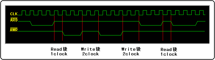
Figure 3.28 Timing when precharge insertion bit is set after reading

* The clock (CLK) in the figure is the internal clock of the SCU.

External weight valid bit in CS0 space ( 4 [bit 28] in Figure 3.24 )
A0EWT (W) A-Bus CS0 External WaiT effective bit
When accessing the CS0 space via A-Bus, weights can be forcibly added by an external signal, but it is a bit that determines whether to enable or disable the processing. 1 is valid and 0 is invalid. When enabled, it will continue to wait while the external weight signal is Low at the point of SCU weight sampling. Figure 3.29 shows the difference in timing charts when external weights are disabled and enabled.

Figure 3.29 Difference in timing due to external weight valid bit setting
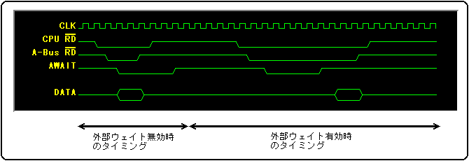
* The clock (CLK) in the figure is the internal clock of the SCU.

Burst cycle weight number setting bit in CS0 space ( 5 to 8 [bit 27 to 24] in Fig. 3.24 )
A0BW3-0 (W) A-Bus CS0 Burst sycle Wait bit3-0
Set the number of waits for one cycle when performing burst access in CS0 space. Table 3.10 shows the setting values.

Table 3.10 CS0 Spatial Burst Cycle Settings
 bit
 Number of weights
 A0BW3
 A0BW2
 A0BW1
 A0BW0
 0
 0
 0
 0
 Do not weight (do not sample weights)
 0
 0
 0
 1
 1 cycle weight
 :
 :
 :
 :
 1
 1
 1
 0
 14 cycle weight
 1
 1
 1
 1
 15 cycle weight

Normal cycle weight number setting bit in CS0 space ( 9 to 12 [bit 23 to 20] in Fig. 3.24 )
A0NW3-0 (W) A-Bus CS0 Normal cycle Wait bit3-0
In CS0 space, set the number of waits for one cycle when performing normal access. Table 3.11 shows the setting values.

Table 3.11 CS0 spatial normal cycle setting values
 bit
 Number of weights
 A0NW3
 A0NW2
 A0NW1
 A0NW0
 0
 0
 0
 0
 Do not weight (do not sample weights)
 0
 0
 0
 1
 1 cycle weight
 :
 :
 :
 :
 1
 1
 1
 0
 14 cycle weight
 1
 1
 1
 1
 15 cycle weight

Burst length setting bit in CS0 space ( 13 to 14 [bit 19 to 18] in Fig. 3.24 )
A0LN1-0 (W) A-Bus CS0 burst LeNgth bit1-0
In CS0 space, specify the length (boundary) to access when burst access is performed. Table 3.12 shows the length settings.

Table 3.12 CS0 Spatial Burst Length Settings
 bit
 Access setting value
 A0LN1
 A0LN0
 0
 0
 Do not burst access
 0
 1
 4 address burst access
 1
 0
 256 address burst access
 1
 1
 No boundaries

Bus size setting bit in CS0 space ( 15 [bit 16] in Fig. 3.24 )
A0SZ (W) A-Bus CS0 bus SiZe bit
Set the A-Bus bus size in CS0 space. Table 3.13 shows the setting values.

Table 3.13 CS0 spatial bus size settings
 A0SZ
 Bus size setting
 0
 Specify 16-bit bus
 1
 Specify 8 bit bus

Post-write precharge insertion bit in CS1 space ( 17 [bit 14] in Figure 3.24 )
A1WPC (W) A-Bus CS1 after Write Pre-Charge insert bit
After writing the data to the CS1 space, you can insert the unprocessed state for one clock. This bit determines whether the process is enabled or disabled. 1 is valid and 0 is invalid. This bit does not affect the behavior after reading. See Figure 3.27 for the behavior when this bit is set.

Post-read precharge insertion bit in CS1 space ( 18 [bit 13] in Figure 3.24 )
A1RPC (W) A-Bus CS1 Read Pre-Charge insert bit
After reading the data in CS1 space, you can insert the unprocessed state for one clock. This bit determines whether the process is enabled or disabled. 1 is valid and 0 is invalid. This bit does not affect the behavior after writing. See Figure 3.28 for the behavior when this bit is set.

External weight valid bit in CS1 space ( 19 [bit 12] in Figure 3.24 )
A1EWT (W) A-Bus CS1 External WaiT effective bit
When accessing the CS1 space via A-Bus, weights can be forcibly added by an external signal, but it is a bit that determines whether to enable or disable the processing. 1 is valid and 0 is invalid. When enabled, it continues to wait while the external signal is Low. See Figure 3.29 for the difference in timing charts when external weights are disabled and enabled.

Burst cycle weight number setting bit in CS1 space ( 20 to 23 [bit 11 to 8] in Fig. 3.24 )
A1BW3-0 (W) A-Bus CS1 Burst sycle Wait bit3-0
Set the number of waits for one cycle when performing burst access in CS1 space. Table 3.14 shows the setting values.

Table 3.14 CS1 Spatial Burst Cycle Settings
 bit
 Number of weights
 A1BW3
 A1BW2
 A1BW1
 A1BW0
 0
 0
 0
 0
 Do not weight (do not sample weights)
 0
 0
 0
 1
 1 cycle weight
 :
 :
 :
 :
 1
 1
 1
 0
 14 cycle weight
 1
 1
 1
 1
 15 cycle weight

Normal cycle weight number setting bit in CS1 space ( 24 to 27 [bit 7 to 4] in Fig. 3.24 )
A1NW3-0 (W) A-Bus CS1 Normal cycle Wait bit3-0
In the CS1 space, set the number of waits for one cycle when performing normal access. Table 3.15 shows the setting values.

Table 3.15 CS1 spatial normal cycle setting values
 bit
 Number of weights
 A1NW3
 A1NW2
 A1NW1
 A1NW0
 0
 0
 0
 0
 Do not weight (do not sample weights)
 0
 0
 0
 1
 1 cycle weight
 :
 :
 :
 :
 1
 1
 1
 0
 14 cycle weight
 1
 1
 1
 1
 15 cycle weight

Burst length setting bits in CS1 space ( 28 to 29 [bits 3 to 2] in Fig. 3.24 )
A1LN1-0 (W) A-Bus CS1 burst LeNgth bit1-0
In CS1 space, specify the length (boundary) to access when burst access is performed. Table 3.16 shows the length settings.

Table 3.16 CS1 Spatial Burst Length Settings
 bit
 Access setting value
 A1LN1
 A1LN0
 0
 0
 Do not burst access
 0
 1
 4 address burst access
 1
 0
 256 address burst access
 1
 1
 No boundaries

Bus size setting bit in CS1 space ( 30 [bit 0] in Fig. 3.24 )
A1SZ (W) A-Bus CS1 bus SiZe bit
Set the A-Bus bus size in CS1 space. Table 3.17 shows the setting values.

Table 3.17 CS1 spatial bus size settings
 A1SZ
 Bus size setting
 0
 Specify 16-bit bus
 1
 Specify 8 bit bus

Post-write precharge insertion bit in CS2 space ( 2 [bit 30] in Figure 3.25 )
A2WPC (W) A-Bus CS2 after Write Pri-Charge insert bit
After writing the data to CS2 space, you can insert the unprocessed state for one clock. This bit determines whether the process is enabled or disabled. 1 is valid and 0 is invalid. This bit does not affect the behavior after reading. See Figure 3.27 for the behavior when this bit is set.

Post-read precharge insertion bit in CS2 space ( 3 [bit 29] in Figure 3.25 )
A2RPC (W) A-Bus CS2 Read Pri-Charge insert bit
After reading the data in CS2 space, you can insert the unprocessed state for one clock. This bit determines whether the process is enabled or disabled. 1 is valid and 0 is invalid. This bit does not affect the behavior after writing. See Figure 3.28 for the behavior when this bit is set.

External weight valid bit in CS2 space ( 4 [bit 28] in Figure 3.25 )
A2EWT (W) A-Bus CS2 External WaiT effective bit
When accessing the CS2 space via A-Bus, weights can be forcibly added by an external signal, but it is a bit that determines whether to enable or disable the processing. 1 is valid and 0 is invalid. When enabled, it continues to wait while the external signal is Low. See Figure 3.29 for the difference in timing charts when external weights are disabled and enabled.

Burst length setting bit in CS2 space ( 5 to 6 [bit 19 to 18] in Fig. 3.25 )
A2LN1-0 (W) A-Bus CS2 burst LeNgth bit1-0
In CS2 space, specify the length (boundary) to access when burst access is performed. Table 3.18 shows the length settings.

Table 3.18 CS2 Spatial Burst Length Settings
 bit
 Access setting value
 A2LN1
 A2LN0
 0
 0
 Do not burst access
 0
 1
 4 address burst access
 1
 0
 256 address burst access
 1
 1
 No boundaries

Bus size setting bit in CS2 space ( 7 [bit 16] in Fig. 3.25 )
A2SZ (W) A-Bus CS2 bus SiZe bit
Set the A-Bus bus size in CS2 space. Table 3.19 shows the setting values.

Table 3.19 CS2 spatial bus size settings
 A2SZ
 Bus size setting
 0
 Specify 16-bit bus
 1
 Specify 8 bit bus

Precharge insertion bit after writing in spare space ( 9 [bit 14] in Fig. 3.25 )
A3WPC (W) A-Bus CS3 after Write Pri-Charge insert bit
After writing the data to the spare space, you can insert the unprocessed state for one clock. This bit determines whether the process is enabled or disabled. 1 is valid and 0 is invalid. This bit does not affect the behavior after reading. See Figure 3.27 for the behavior when this bit is set.

Precharge insertion bit after read of spare space ( 10 [bit 13] in Fig. 3.25 )
A3RPC (W) A-Bus CS3 Read Pri-Charge insert bit
After reading the data in the spare space, you can insert the unprocessed state for one clock. This bit determines whether the process is enabled or disabled. 1 is valid and 0 is invalid. This bit does not affect the behavior after writing. See Figure 3.28 for the behavior when this bit is set.

External weight valid bit in spare space ( 11 [bit 12] in Figure 3.25 )
A3EWT (W) A-Bus CS3 External WaiT effective bit
When accessing the spare space via A-Bus, a wait can be forcibly added by an external signal, but it is a bit that determines whether to enable or disable the processing. 1 is valid and 0 is invalid. When enabled, it continues to wait while the external signal is Low. See Figure 3.29 for the difference in timing charts when external weights are disabled and enabled.

Burst cycle weight number setting bit in spare space ( 12 to 15 [bit 11 to 8] in Fig. 3.25 )
A3BW3-0 (W) A-Bus CS3 Burst sycle Wait bit3-0
In the spare space, set the number of waits for one cycle when performing burst access. Table 3.20 shows the setting values.

Table 3.20 Spare space burst cycle settings
 bit
 Number of weights
 A3BW3
 A3BW2
 A3BW1
 A3BW0
 0
 0
 0
 0
 Do not weight (do not sample weights)
 0
 0
 0
 1
 1 cycle weight
 :
 :
 :
 :
 1
 1
 1
 0
 14 cycle weight
 1
 1
 1
 1
 15 cycle weight

Normal cycle weight number setting bit in spare space ( 16 to 19 [bit 7 to 4] in Fig. 3.25 )
A3NW3-0 (W) A-Bus CS3 Normal cycle Wait bit3-0
In the spare space, set the number of waits for one cycle when performing normal access. Table 3.21 shows the setting values.

Table 3.21 Spare space normal cycle setting values
 bit
 Number of weights
 A3NW3
 A3NW2
 A3NW1
 A3NW0
 0
 0
 0
 0
 Do not weight (do not sample weights)
 0
 0
 0
 1
 1 cycle weight
 :
 :
 :
 :
 1
 1
 1
 0
 14 cycle weight
 1
 1
 1
 1
 15 cycle weight

Burst length setting bit in spare space ( 20 to 21 [bit 3 to 2] in Fig. 3.25 )
A3LN1-0 (W) A-Bus CS3 burst LeNgth bit1-0
In the spare space, specify the length (boundary) to access when burst access is performed. Table 3.22 shows the length settings.

Table 3.22 Spare space burst length settings
 bit
 Access setting value
 A3LN1
 A3LN0
 0
 0
 Do not burst access
 0
 1
 4 address burst access
 1
 0
 256 address burst access
 1
 1
 No boundaries

Spare space bus size setting bit ( 22 [bit 0] in Fig. 3.25 )
A3SZ (W) A-Bus CS3 bus SiZe bit
Set the A-Bus bus size in the spare space. Table 3.23 shows the setting values.

Table 3.23 Spare space bus size settings
 A3SZ
 Bus size setting
 0
 Specify 16-bit bus
 1
 Specify 8 bit bus

◆ A-Bus refresh register

Figure 3.30 shows the details of the A-Bus refresh register.

Figure 3.30 A-Bus refresh register (register: AREF) initial value 00000010H
bit
 31
 twenty four
 twenty three
 16
 15
 8
 7
 0
25FE00A0 1 2 3 4 5

A-Bus refresh output valid bit ( 1 [bit 4] in Figure 3.30 )
ARFEN (W) A-Bus ReFresh ENable bit
Enables A-Bus refresh cycle output. Valid with "1". The initial value of this bit at power-on reset is "1".

The A-Bus refresh output valid bit is prohibited from being changed by the user.

A-Bus refresh weight number setting bit ( 2 to 5 [bit 3 to 0] in Fig. 3.30 )
ARWT3-0 (W) A-Bus Refresh WaiT bit3-0
Sets the number of A-Bus refresh cycle waits. Table 3.24 shows the details.

Table 3.24 Number of A-Bus refresh weights
 bit
 Number of weights
 ARWT3
 ARWT2
 ARWT1
 ARWT0
 0
 0
 0
 0
 Do not wait
 0
 0
 0
 1
 1 cycle weight
 :
 :
 :
 :
 1
 1
 1
 0
 14 cycle weight
 1
 1
 1
 1
 15 cycle weight

◆ Restrictions when using A-Bus

Precautions when using flash memory on A-Bus
When using flash memory on A-Bus, if the software waits between write and write, interrupts or DMA will occur in the middle, and operation is guaranteed if the distance between write and write exceeds the specifications of flash memory and becomes long. Will not be.
Therefore, if you are using flash memory under the above conditions, you should disable interrupts and DMA.

Similar precautions should be taken when using power memory.

Restrictions when using an area other than ACS2 of A-Bus as an 8-bit bus
When using an area other than CS2 of A-Bus as an 8-bit bus, if you write a bus to the 8-bit bus area, an abnormal cycle may occur in which only ACS becomes active.
This occurs when a 16-bit bus area is read or written and then byte-written to the address 4n + 2 (n is an integer) of the 8-bit bus area. , ARD and AWRO, AWR1 are "inactive" and the data bus is "output".
In order to prevent the occurrence of such an abnormal state, if an area other than CS2 of A-Bus is assigned to the 8-bit bus, one of the following restrictions is required.

  1. When the byte write to the 8-bit bus area and the read or write to the 16-bit bus area are alternately performed, it is necessary that the interrupt DMA or the like does not occur unexpectedly.
    Disable interrupts and DMA

  2. Only word lights can be used to light the 8-bit bus area.

  3. Write read only to the 8-bit bus area.

  4. Writing to the address of 4n + 2 (n is an integer) to the 8-bit bus is prohibited.

BackForward
HARDWARE ManualSCU User's Manual3.1 Register List
Copyright SEGA ENTERPRISES, LTD., 1997