HARDWARE ManualSMPC User's Manual
BackForward
SMPC User's Manual / Chapter 1 Overview

■ 1.2 SH-2 interface

◆ SH-2 interface register

The SH-2 interface register is a register used for commands from the SH-2, command parameter setting and status display, and result parameter output.
Figure 1.3 shows the address map of the SH-2 interface register.

Figure 1.3 SH-2 Interface Register Address Map
      bit70 
         ┌────────────────┐ 
2010001FH  COMREG │ W 
         └────────────────┘ 
      bit70 
         ┌────────────────┐ 
20100061H │ S R │ R 
         └────────────────┘ 
      bit70 
         ┌─┬─┬─┬─┬─┬─┬─┬──┐ 
20100063H │ │ SF │ R / W
         └─┴─┴─┴─┴─┴─┴─┴──┘ 
      bit70 
         ┌────────────────┐┐ 
20100001H  IREG0 │ │ 
         ├────────────────┤│ 
20100003H │ IREG1 │ │ 
         ├────────────────┤│ 
20100005H  IREG2 │ │ 
         ├────────────────┤│ 
20100007H  IREG3 │ W 
         ├────────────────┤│ 
20100009H│ IREG4 ││ 
         ├────────────────┤│ 
2010000BH  IREG5 │ │ 
         ├────────────────┤│ 
2010000DH  IREG6 │ │ 
         └────────────────┘┘ 
      bit70 bit7 0
         ┌────────────────┐┐┌────────────────┐┐
20100021H  ORE G0  │ 20100041H │ ORE G16 │ │
         ├────────────────┤│├────────────────┤│
20100023H  ORE G1  │ 20100043H │ ORE G17 │ │
         ├────────────────┤│├────────────────┤│
20100025H  ORE G2  │ 20100045H │ ORE G18 │ │
         ├────────────────┤│├────────────────┤│
20100027H  ORE G3  │ 20100047H │ ORE G19 │ │
         ├────────────────┤│├────────────────┤│
20100029H  ORE G4  │ 20100049H │ ORE G20 │ │
         ├────────────────┤│├────────────────┤│
2010002BH  ORE G5 │ │ 2010004 BH │ ORE G21 │ │
         ├────────────────┤│├────────────────┤│
2010002DH  ORE G6 │ │ 2010004 DH │ ORE G22 │ │
         ├────────────────┤│├────────────────┤│
2010002FH  ORE G7 │ │ 2010004 FH │ ORE G23 │ │
         ├────────────────┤R ├────────────────┤R
20100031H  ORE G8  │ 20100051H │ ORE G24 │ │
         ├────────────────┤│├────────────────┤│
20100033H  ORE G9  │ 20100053H │ ORE G25 │ │
         ├────────────────┤│├────────────────┤│
20100035H  ORE G10  │ 20100055H │ ORE G26 │ │
         ├────────────────┤│├────────────────┤│
20100037H  ORE G11  │ 20100057H │ ORE G27 │ │
         ├────────────────┤│├────────────────┤│
20100039H  ORE G12  │ 20100059H │ ORE G28 │ │
         ├────────────────┤│├────────────────┤│
2010003BH  ORE G13 │ │ 2010005 BH │ ORE G29 │ │
         ├────────────────┤│├────────────────┤│
2010003DH  ORE G14 │ │ 2010005 DH │ ORE G30 │ │
         ├────────────────┤│├────────────────┤│
2010003FH  ORE G15 │ │ 2010005 FH │ ORE G31 │ │
         └────────────────┘┘└────────────────┘┘
         ★ Only byte access is possible for all registers

The details of the SH-2 interface register are shown below.

COMREG (W): COMmand REGister
An 8-bit register for receiving various commands from SH-2. SMPC parses and executes the command as soon as it is written. SMPC has reset system management commands, non-reset system management commands, and RTC commands. Please access bytes from SH-2.

SR (R): Status Register
An 8-bit register for SMPC to display the status after executing a command. It is possible to always read from SH-2 regardless of command issuance. At the time of peripheral control, various statuses of peripheral control are shown. Please access bytes from SH-2.

SF (R / W): Status Flag
A flag for managing command issuance. The flag is set by SH-2 before the command is issued, and SMPC resets when the command ends. From SH-2, only set is possible. When setting, please light 01H. At the time of reading, it is undefined except for bit0. You can use this flag to manage the double issuance of commands. Please access bytes from SH-2.

IREG0 to IREG6 (W): Input REGister 0 to 6
An 8-bit register for receiving command parameters from SH-2. Seven IREGs are available for SMPC. Please access bytes from SH-2.

OREG0 to OREG31 (R): Output REGister 0 to 31
This is an 8-bit register for outputting result parameters and peripheral data to SH-2. The SMPC has 32 OREGs, which are used to acquire the cartridge code, area code, peripheral data, current time, etc. Please access bytes from SH-2.

◆ Parallel I / O register

A register for controlling the peripheral interface in the SMPC. Figure 1.4 shows the address map of the parallel I / O registers. Note that the write-only register cannot be read.

Figure 1.4 Parallel I / O Register Address Map

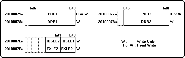
* Only byte access is possible for all registers!

DDR1 (W): Data Direction Register 1
This is a 7-bit register that sets the input / output direction of peripheral port 1 (P1) in bit units. Writing "0" to each bit sets it to input, and writing "1" sets it to output. Please access bytes from SH-2.

DDR2 (W): Data Direction Register 2
This is a 7-bit register that sets the input / output direction of peripheral port 2 (P2) in bit units. Writing "0" to each bit sets it to input, and writing "1" sets it to output. Please access bytes from SH-2.

Table 1.3 DDR function settings
Set value function
0 Set to input (initial value)
1 Set to output

PDR1 (R or W): Port Data Register 1
PDR1 is a 7-bit register that stores data for peripheral port 1 (P1). Whether each bit of PDR1 is an input port or an output port depends on the DDR1 settings. By writing data to this register, the terminal state of the port set for output can be changed. By reading this register, the terminal status of the port set for input can be read. Also, for the port set for output, the value written to PDR1 is read, not the state of the terminal. Please access bytes from SH-2.

PDR2 (R or W): Port Data Register 2
PDR2 is a 7-bit register that stores data on peripheral port 2 (P2). Whether each bit of PDR2 is an input port or an output port depends on the DDR2 settings. By writing data to this register, the terminal state of the port set for output can be changed. By reading this register, the terminal status of the port set for input can be read. Also, for the port set for output, the value written to PDR2 is read, not the state of the terminal. Please access bytes from SH-2.

IOSEL1 (W): I / O SELect 1
Set peripheral port 1 (P1) to SMPC control mode or SH-2 direct mode. Writing "0" sets the SMPC control mode, and writing "1" sets the SH-2 direct mode. Please access bytes from SH-2.

IOSEL2 (W): I / O SELect 2
Set peripheral port 2 (P2) to SMPC control mode or SH-2 direct mode. Writing "0" sets the SMPC control mode, and writing "1" sets the SH-2 direct mode. Please access bytes from SH-2.

Table 1.4 IOSEL features
Set value function
0 Set to SMPC control mode (initial value)
1 Set to SH-2 direct mode

See Chapter 3 for details on each mode.

Use of SH-2 direct mode is prohibited.
(Excluding peripherals using SH-2 direct mode)

EXLE1 (W): EXternal Latch Enable 1
A bit that sets whether bit 6 of peripheral port 1 (P1) is used as an input for a PAD interrupt or an external latch for VDP2. Writing "0" disables it and bit 6 of peripheral port 1 is set as a normal I / O port. Writing "1" enables it, and bit 6 of peripheral port 1 can be used as a PAD interrupt input or an external latch input of VDP2. Please access bytes from SH-2.

EXLE2 (W): EXternal Latch Enable 2
A bit that sets whether bit 6 of peripheral port 2 (P2) is used as an input for a PAD interrupt or an external latch for VDP2. Writing "0" disables it and bit 6 of peripheral port 2 is set as a normal I / O port. Writing "1" enables it, and bit 6 of peripheral port 2 can be used as a PAD interrupt input or an external latch input of VDP2. Please access bytes from SH-2.

Table 1.5 EXLE function
Set value function
0 Disable (initial value)
1 Enable

EXLE is multiplexed on bit 6 of the I / O port. Therefore, when using EXLE, it is necessary to set bit 6 of DDR1 / DDR2 to the input.
(See VDP2 External Latch Function and SCU PAD Interrupt.)

BackForward
HARDWARE ManualSMPC User's Manual
Copyright SEGA ENTERPRISES, LTD., 1997