 ★ HARDWARE Manual ★ SCU User's Manual ★ 3.1 Register List
| bit | 31 | twenty four | twenty three | 16 | 15 | 8 | 7 | 0 | ||||||||||||||||||||||||
25FE0000 (level 0) 25FE0020 (level 1) 25FE0040 (level 2) | − | − | − | − | − | 1 | 2 | 3 | 4 | 5 | 6 | 7 | 8 | 9 | Ten | 11 | 12 | 13 | 14 | 15 | 16 | 17 | 18 | 19 | 20 | twenty one | twenty two | twenty three | twenty four | twenty five | 26 | 27 |
| bit | 31 | twenty four | twenty three | 16 | 15 | 8 | 7 | 0 | ||||||||||||||||||||||||
25FE0004 (level 0) 25FE0024 (level 1) 25FE0044 (level 2) | − | − | − | − | − | 1 | 2 | 3 | 4 | 5 | 6 | 7 | 8 | 9 | Ten | 11 | 12 | 13 | 14 | 15 | 16 | 17 | 18 | 19 | 20 | twenty one | twenty two | twenty three | twenty four | twenty five | 26 | 27 |
| bit | 31 | twenty four | twenty three | 16 | 15 | 8 | 7 | 0 | ||||||||||||||||||||||||
25FE0008 (level 0) | − | − | − | − | − | − | − | − | − | − | − | − | 1 | 2 | 3 | 4 | 5 | 6 | 7 | 8 | 9 | Ten | 11 | 12 | 13 | 14 | 15 | 16 | 17 | 18 | 19 | 20 |
| bit | 31 | twenty four | twenty three | 16 | 15 | 8 | 7 | 0 | ||||||||||||||||||||||||
25FE0028 (level 1) 25FE0048 (level 2) | − | − | − | − | − | − | − | − | − | − | − | − | − | − | − | − | − | − | − | − | 1 | 2 | 3 | 4 | 5 | 6 | 7 | 8 | 9 | Ten | 11 | 12 |
 | Do not read the number of transferred bytes in the DMA transfer register |
| bit | 31 | twenty four | twenty three | 16 | 15 | 8 | 7 | 0 | ||||||||||||||||||||||||
25FE000C (level 0) 25FE002C (Level 1) 25FE004C (level 2) | − | − | − | − | − | − | − | − | − | − | − | − | − | − | − | − | − | − | − | − | − | − | − | 1 | − | − | − | − | − | 2 | 3 | 4 |
DxRA (x = 2-0) | Contents |
0 | Do not add. |
1 | Add 4 bytes. |
DxWA (x = 2-0) | Contents |
000B | Do not add |
001B | Add 2 bytes |
010B | Add 4 bytes |
011B | Add 8 bytes |
100B | Add 16 bytes |
101B | Add 32 bytes |
110B | Add 64 bytes |
111B | Add 128 bytes |
Figure 3.6 Communication unit between SCU and processor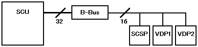
Figure 3.7 Specific example of transfer between SCU and processor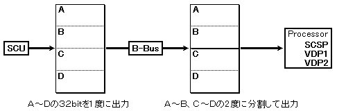
Figure 3.8 Specifying the write-out address addition value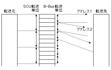
| External area 4 area (A-Bus I / O area) → | 0b and 1b can be set |
| Other → | Only 1b can be set |
| WORKRAM-H → | 010b can be set |
| External areas 1-3 areas → | 010b can be set |
| External area 4 area (A-Bus I / O area) → | 000b,010b can be set |
| VDP1, VDP2, SCSP → | All settings are possible |
| External area 1-4 area (A-Bus) → | 010b can be set |
| VDP1, VDP2, SCSP (B-Bus) → | 001b can be set |
| WORKRAM-H (C-Bus) → | 010b can be set |
| bit | 31 | twenty four | twenty three | 16 | 15 | 8 | 7 | 0 | ||||||||||||||||||||||||
25FE0010 (level 0) 25FE0030 (level 1) 25FE0050 (level 2) | − | − | − | − | − | − | − | − | − | − | − | − | − | − | − | − | − | − | − | − | − | − | − | 1 | − | − | − | − | − | − | − | 2 |
| bit | 31 | twenty four | twenty three | 16 | 15 | 8 | 7 | 0 | ||||||||||||||||||||||||
25FE0014 (level 0) 25FE0034 (level 1) 25FE0054 (level 2) | − | − | − | − | − | − | − | 1 | − | − | − | − | − | − | − | 2 | − | − | − | − | − | − | − | 3 | − | − | − | − | − | 4 | 5 | 6 |
Start factor bit (x = 2-0) | Trigger factor | ||
DxFT2 | DxFT1 | DxFT0 | |
0 | 0 | 0 | Allow set of bits and V-blank-IN signal reception |
0 | 0 | 1 | Allow set of bits and V-blank-OUT signal reception |
0 | 1 | 0 | Allow set of bits and H-blank-IN signal reception |
0 | 1 | 1 | Allow set of bits and timer 0 signal reception |
1 | 0 | 0 | Allow set of bits and timer 1 signal reception |
1 | 0 | 1 | Allow set of bits and sound-Req signal reception |
1 | 1 | 0 | Allow set of bits and receive sprite drawing end signal |
1 | 1 | 1 | Set of allow bits and set of DMA start bits |
★ HARDWARE Manual ★ SCU User's Manual ★ 3.1 Register List